【ASEMI】Voltage Stress Analysis of "Key Components" of SMPS
Return ListSource:Asemi Date:2013.12.31 Read:0
Voltage Stress Analysis of "Key Components" of SMPS
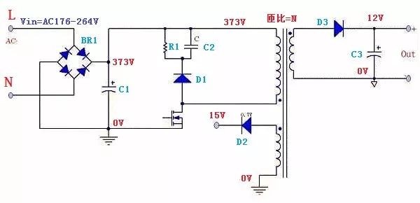
Before setting up the test and calculation, first set it up, the circuit diagram is designed as above, the main parameters are as follows:
Input voltage: Vin=AC176-264V
Output voltage: Vout=12V
Vcc voltage: Vcc=15V
Transformer turns ratio: N
The stress calculation is performed on the rectifier bridge components in the picture below.
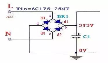
The rectifier bridge is composed of four diodes as shown in the figure: d1, d2, d3, d4
Should be bad when the input voltage max, that is, Vin = 264Vac
Therefore, the voltage at both ends of C1 is 373V.
The input voltage waveform is as follows:
When the input voltage is in the positive half cycle, the diodes d1 and d4 in the BR1 body are not subjected to high voltage, d2 and d3 are cut off to withstand high voltage, d2 voltage stress is b point potential minus c point potential, d3 voltage stress is a point potential Subtract the d point potential.
The potentials of the positive half-cycles a, b, c, and d are 373V, 373V, 0V, 0V with respect to the large capacitance.
D2 stress = b-c = 373V - 0V = 373V
D3 stress = a-d = 373V-0V = 373V
When the input voltage enters the negative half cycle, the stress of d1 and d4 is 373V.
That is, the working stress of the rectifier bridge in the circuit is 373V.
Since the switching power supply needs to do the lightning surge test, the general rectifier bridge selects the 1000V rectifier bridge.
ASEMI TECH
will be better


 Hotline


