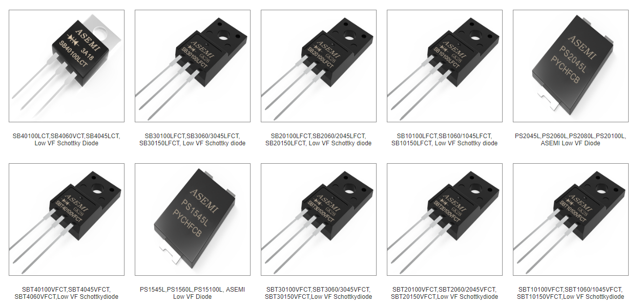
ASEMI Low Dropout Diode Process Technology
Return ListSource:Asemi Date:2017.12.31 Read:0
ASEMI low dropout diode new process technology decomposition
What is the low-voltage drop Schottky diode process technology? Take a look at the ASEMI project to interpret the decomposition of the latest processes.
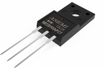
Now with the low-pressure drop Schottky diodes coming out, why is the SBT20100VF being snapped up when it goes out? What is the difference between SBT20100VF and SBT20100UF?
Each generation of low-voltage drop Schottky diodes uses different LOW VF Schottky chip fabrication and finished packaging processes. What are the similarities in the product replacement? ASEMI engineers analyze for you.
The SBT20100VF and SBT20100UF 20A, 100V low forward Schottky products are hot products in 2016. At constant current, the forward voltage drop is lower than conventional Schottky. Using advanced groove manufacturing technology, it can increase the full load efficiency . ASEMI brand low pressure drop Schottky SBT20100VF and SBT20100UF adopt TRENCH advanced technology, the same three feet common structure.
The V of the SBT20100VF stands for the V version of the LOW VF (100V V version VF = 0.63v), while the SBT20100UF stands for the ULTRA LOW VF (100V U version VF = 0.58v).
ASEMI brand of low-voltage drop Schottky diodes, after five years of development, currently has three generations of LOW VF SKY. This product is mainly focused on power conversion efficiency, and achieves ultra-low VF characteristics and fast switching characteristics, which can help your power products improve power switching efficiency and energy saving requirements. ASEMI has a new breakthrough for low-voltage drop Schottky diodes. Technical update.
ASEMI-plane process decomposition (second generation)
The second generation of ASEMI low-voltage drop Schottky uses a planar MOS process to incorporate the MOSFET fabrication process into the Schottky chip process, increasing the density of the chip cell structure, thereby overcoming the traditional Schottky parameters in VF and IR. The balance problem is to maintain the advantages of the traditional Schottky, and to solve the barrier that traditional Schottky encounters in the leakage design.


 Hotline


