ASEMI chip packaging process!
Return ListSource:Asemi Date:2019.07.17 Read:0
Welcome to ASEMI
Today we are going to take you on a tour about the whole process of the chip packaging process of our ASEMI semiconductor chip factory.
Like ASEMI Semiconductor, it is the glass-encapsulated GPP chip, which is the glass passivation process. The glass material is used to make the diaphragm wrap the built-in chip. Compared with the traditional pickling process, the chemical layer of the glass material is more compact. The formation of a tight protective layer protects our chips intact. On the other hand, the packaged chip is also easier to install and transport. It is crucial because the quality of the packaging technology directly affects the performance of the chip itself and the design and manufacture of the PCB (printed circuit board) to which it is connected.
ASEMI Semiconductor warmly reminds you that an important indicator to measure the advancement of a chip packaging technology is the ratio of chip area to package area. The ratio is closer to 1 and the better. The main factors to consider when packaging:
1, the ratio of chip area to package area is to improve packaging efficiency, as close as possible to 1:1;
2, the pin should be as short as possible to reduce the delay, the distance between the pins as far as possible to ensure mutual interference, improve performance;
3. Based on the requirements of heat dissipation, the thinner the package, the better.
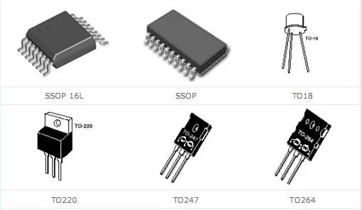
When it comes to packaging, Mainly divided into DIP dual in-line and SMD patch package. In terms of structure, the package has experienced the early transistor TO package developed into a dual in-line package, and then developed a small SOP package, which has developed into a variety of applications. Package: SOJ, TSOP, VSOP, SSOP (reduced SOP), TSSOP and SOT, SOIC, etc. This is the difference from the appearance of the package shape. In addition, from the perspective of material media, there are four kinds of metals, ceramics and plastics.


 Hotline


